As a digital designer, many parts of building a PLL are way outside of my comfort zone. But I thought that getting a PLL IC such as the CD404B was not in the spirit of the project. I also am not sure it would even run slow enough, as I want my clock to run as slow as 1Hz. It is currently not working as intended, although each of the independent circuits appear to be working as expected, so I am working on figuring out the issue. It will currently boost the output clock frequency, but not by the expected amount and phase lock is never achieved.
What is a PLL
A phase lock loop is a system to synthesis one oscillator from another. Feed back from the generated oscillator is used to detect phase differences between the two signals which can be used to update the generated signal to match the reference signal. By altering the feedback it is possible to generate a many different signals from the reference.
A PLL has 4 components: a reference oscillator, a phase detector, a low pass filter, and a Voltage Controlled Oscillator (VCO). Mine also has a clock divider on the the return path from the VCO to the phase detector, which is a common method to boost the output clock frequency. The division factor is programmable, allowing for a range of clock frequencies.
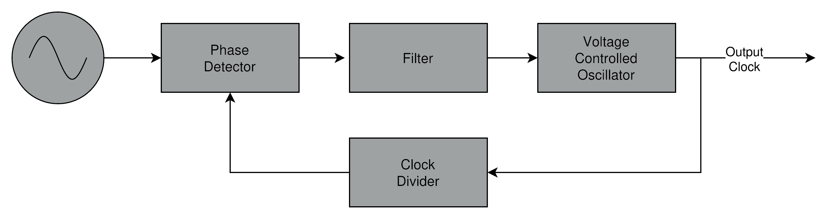
The PLL works by comparing the reference oscillator to the VCO, using the phase detector. The error detected by the phase detector can be used to change the voltage controlling the VCO until the 2 signals are perfectly matched. By passing the VCO output through a divider the phase detector sees a much slower clock. This causes the error to drive the voltage to the VCO higher, until the output frequency is multiplied by the same the factor the divider is performing.
Reference Oscillator
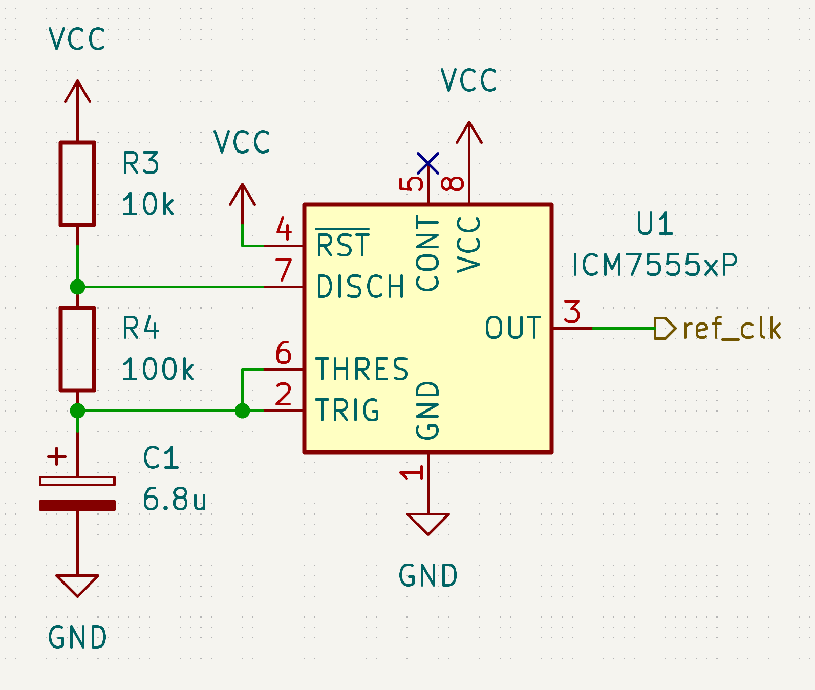
I’m using a 555 IC in it’s astable mode tuned to 1Hz as the reference oscillator. I used the digikey 555 timer calculator to find values for the components that suit.
Phase Detector
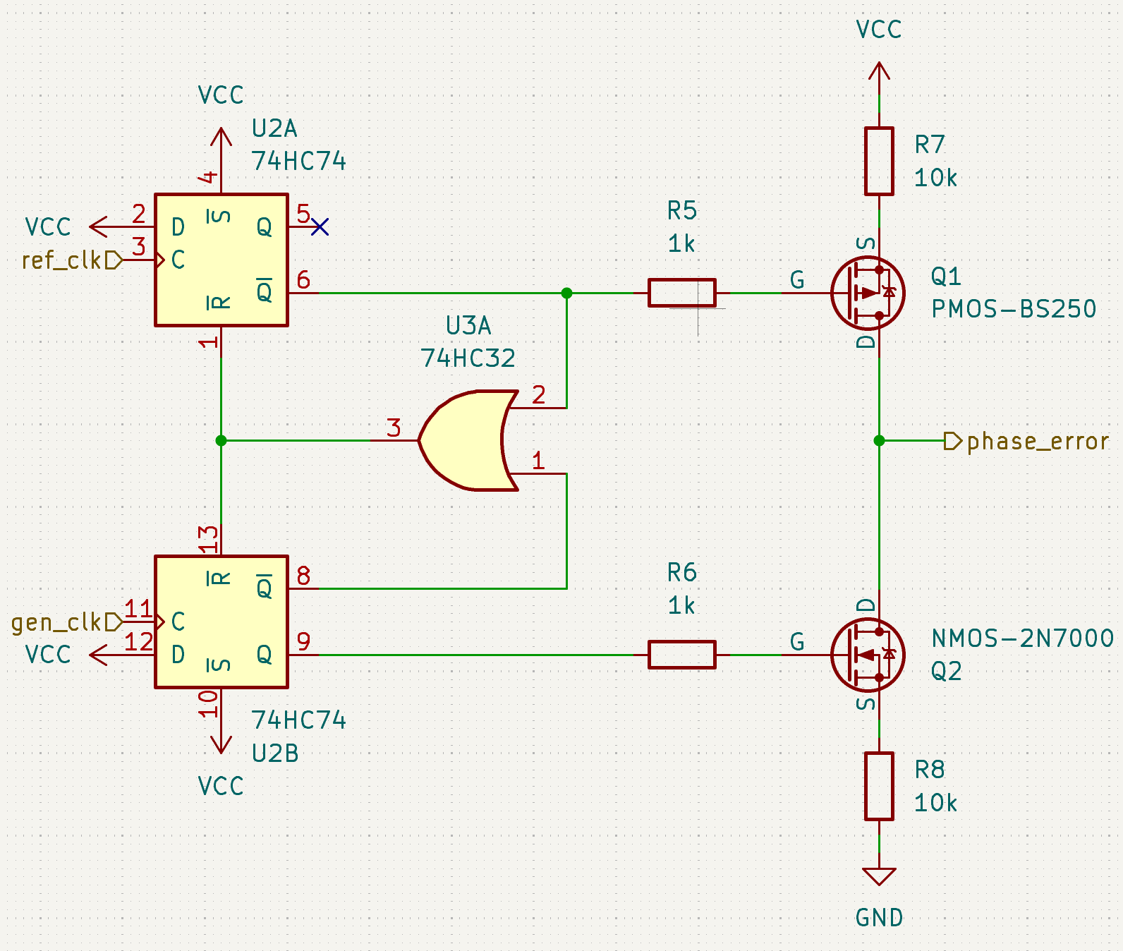
I’m using a type II phase detector. It detects the positive edges of the 2 input clocks. When an edge is detected it opens a MOSFET that pulls the output either high or low depending on which clock was detected. The MOSFET remains open until the a positive edge is detected on the other clock, at which point the phase detector resets, both MOSFETs are closed, and the output voltage is left floating.
Low Pass Filter
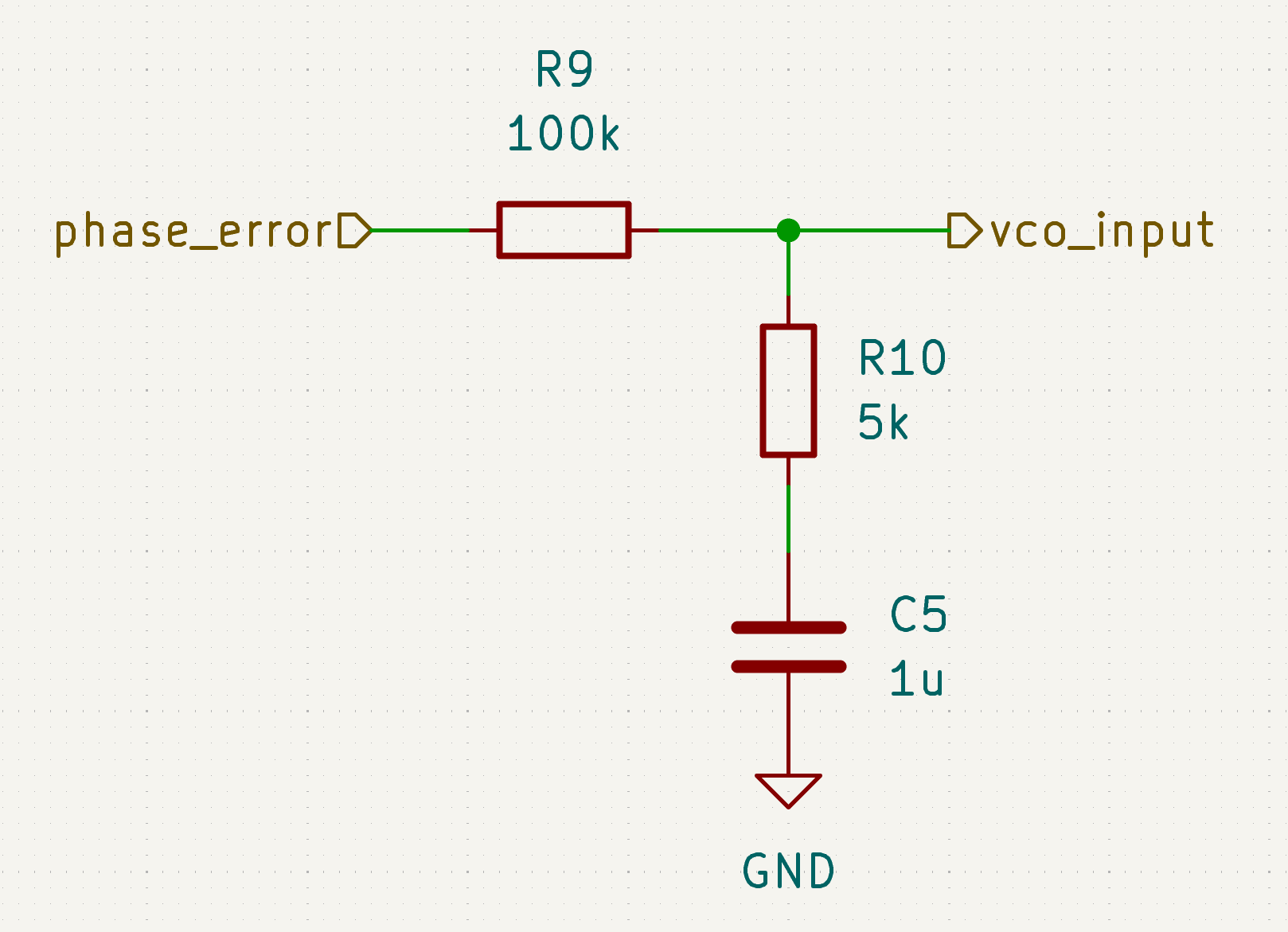
To stop the error immediately driving the VCO to it’s max or min frequency when an edge is detected, a low pass filter is needed to allow the control voltage to change slowly over time. I am using an RC filter with a lag compensator. I picked the values for the RC filter so the -3dB cut off was about 1Hz and the value of the lag compensation resistor out of thin air, and then I experimented with the values until the PLL seemed to be stable and locked in a reasonable time. I think the issues I am having with my current design are either with the values I have selected for the low pass filter or with limits of the mosfets in the phase detector, as it’s seem to have issues getting above about 2V.
Voltage Controlled Oscillator
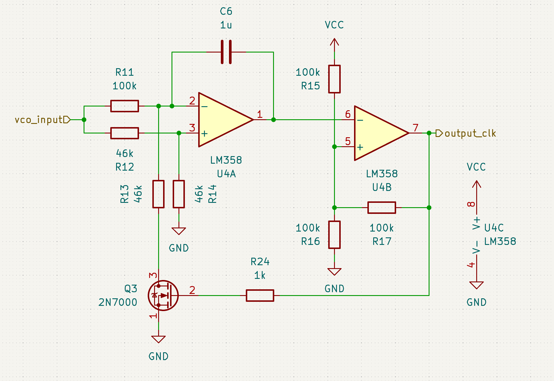
The VCO is made of 2 op-amps. The first generates a triangular wave, which has a frequency that depends on the input voltage. The second is a comparator that converts the triangular wave into a square wave.
Clock divider
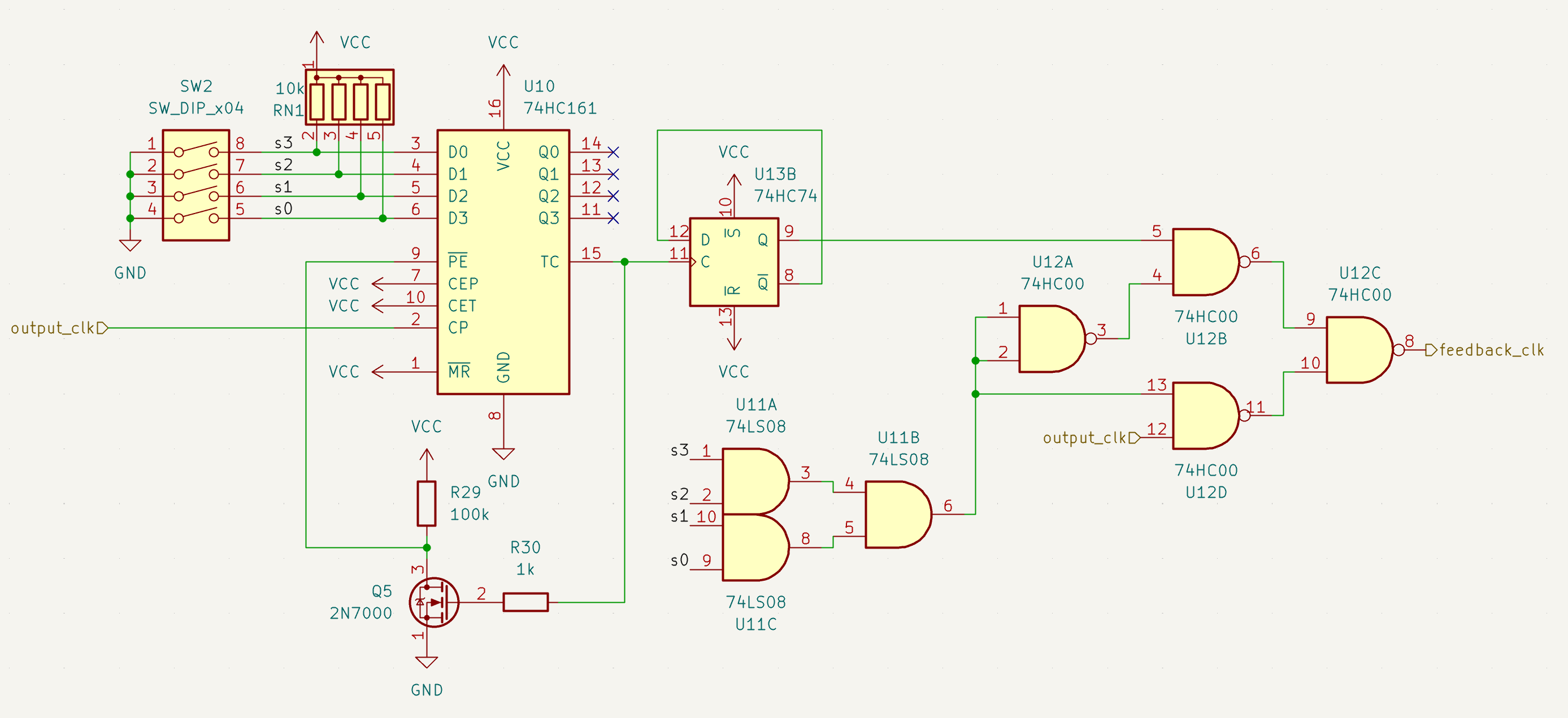
The clock divider includes a counter, a flip flop, and a selector. The counter counts up on each tick of the clock from the VCO. When the counter reaches it’s limit it toggles the flip flop and resets the counter to the value set by the configuration switches. If the switches are all set to zero, the clock from the VCO is passed directly to the phase detector instead of the divided clock.