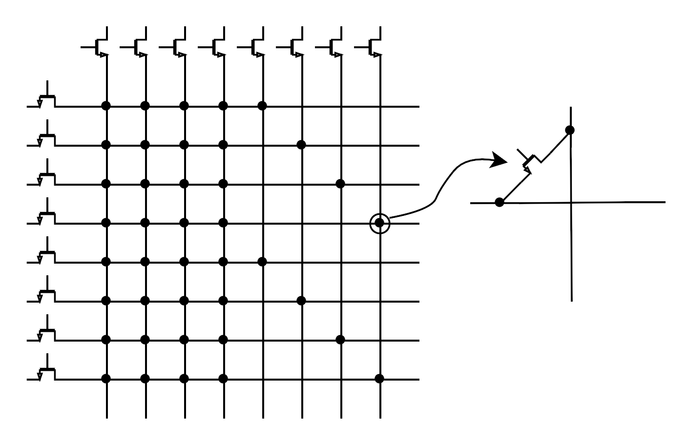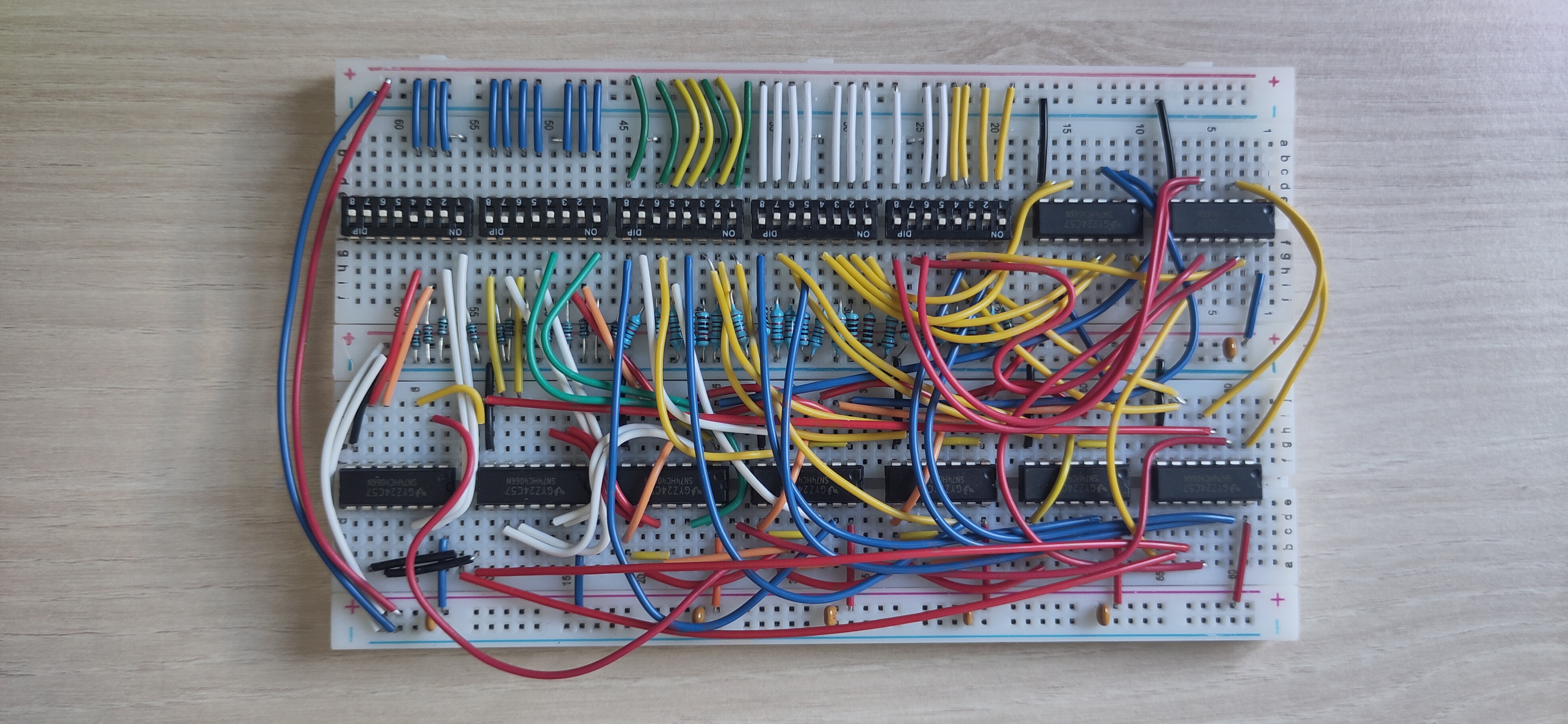
The interconnect is the backbone of an FPGA. It is the wires that connect each of the other modules together and it has to be configurable to allow any two points in the FPGA to be connected together. This causes it take up the majority of the area on the FPGA, even tough it appears relatively simple. My FPGA is based around each module having an 8-bit interface, requiring the interconnect to be an 8x8 grid.
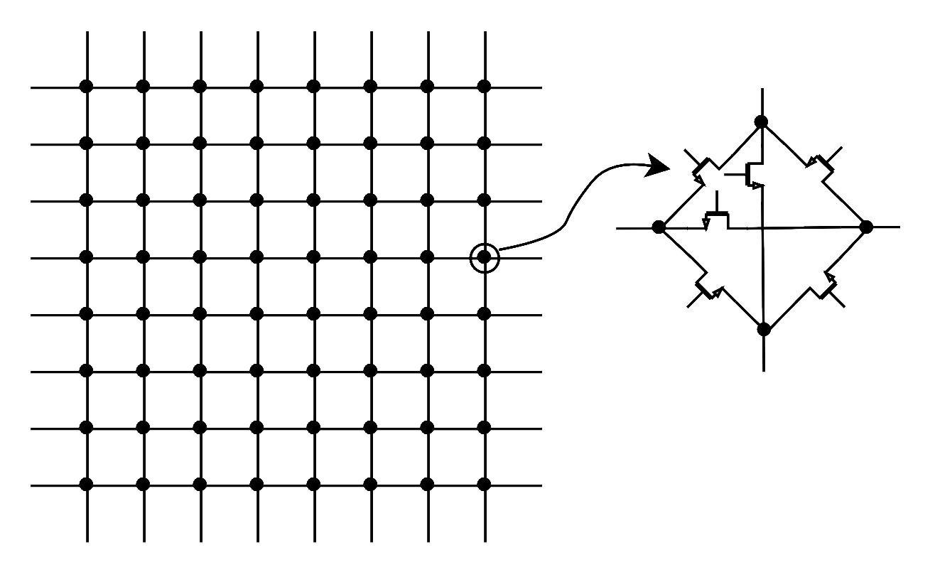
An ideal 8-bit interconnect is able to route any bit from any direction (north/south/east/west) to any of the 8-bits in any of the other directions. This requires an 8x8 matrix, where at each intersections there are 6 pass transistors (at a minimum) to allow each of the possible routing options. This would require 8 x 8 x 6 = 384 transistors plus a configuration switch for each one, which is impractical for my design.
Instead I have built a grid where each of horizontal row is a single wire that can be connected to the each horizontal wire through one switch. I also removed many of the switches on the right hand side of the grid and intend to use these lines for passing signals though the interconnect. The switches here will only be used as backups for when all the left hand wires are in use. Finally I also added switches to the north and west interfaces to prevent signals passing through from one side to the other and on into the next interconnect. These removals will make routing harder and limit designs but seem necessary to me to keep the part count low.