Demos
Done
Example and explanation’s of 3 programs running
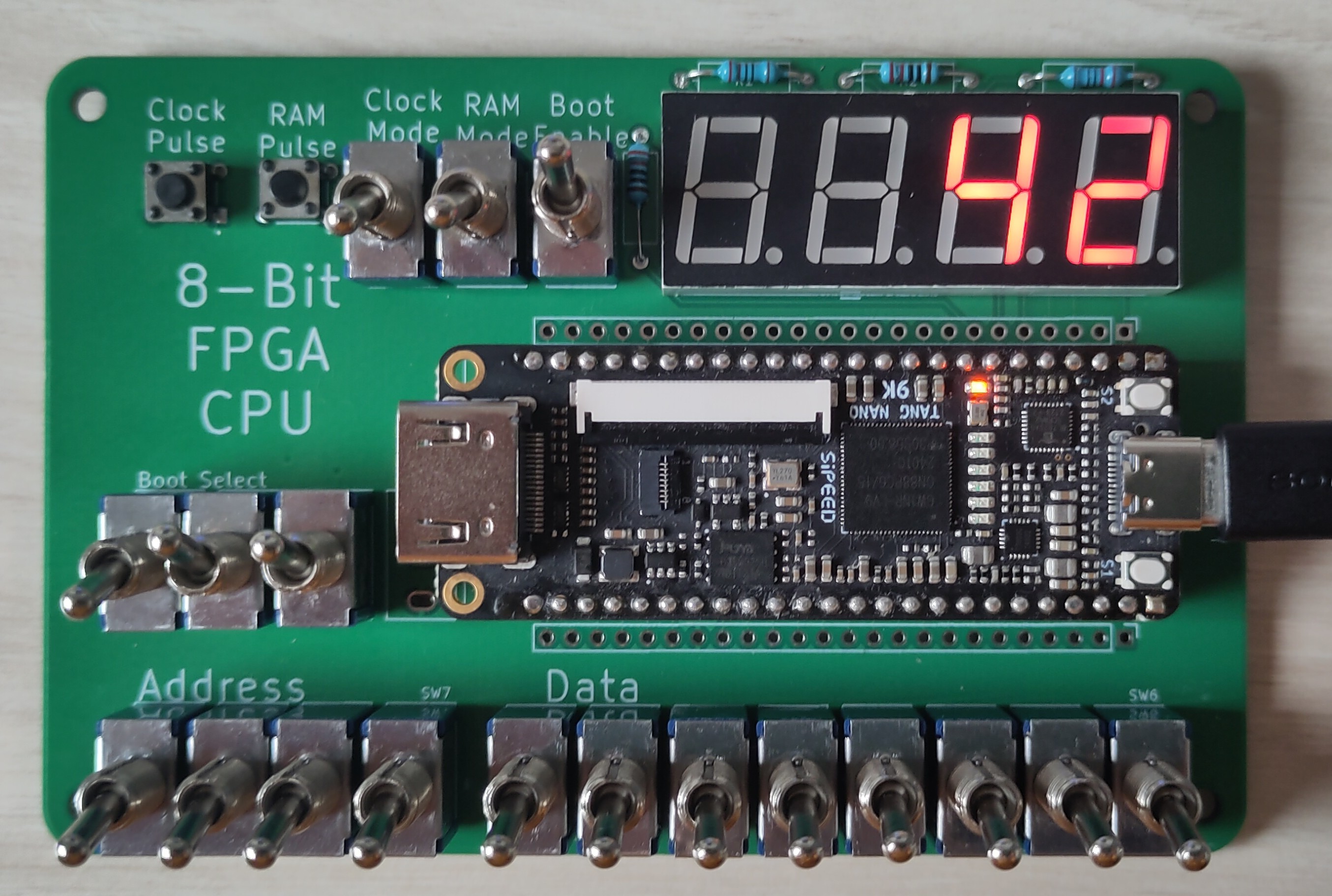
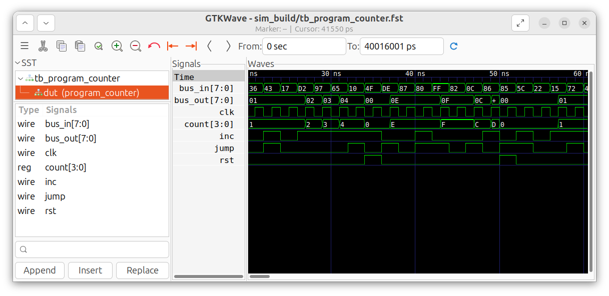
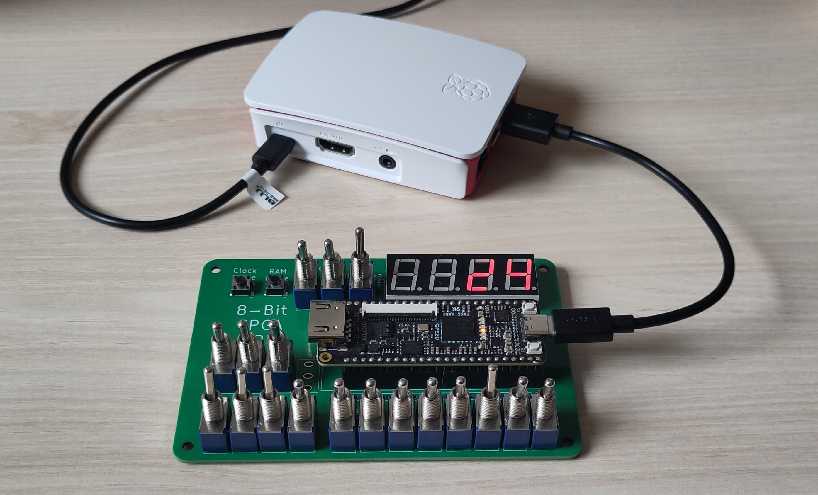
This project was a follow on to my 8-bit PCB CPU. The goal was to cover all the major aspects of FPGA development and brush up on my verilog. I decided to implement the 8-bit CPU as it would be complex first project, but I already knew how it should work so it shouldn’t be to challenging. I used PYUVM to validate each of the modules and created a simple build system using open source tools to quickly get the design on to the FPGA. I used a Tang Nano 9k development board, which uses the GW1NR-9 FPGA from Gowin.
All of the code is available on GitHub.
I made the following 3 major changes to the design of the 8-bit CPU.
The Tang Nano does not support tri-state buffers or bidirectional wires (at least as far as I can tell after far too much debugging), so the bus had to be redesigned. I created a simple bus module that can take a number of input data lanes and a control signal for each lane. It would the output the data based on which control signal was set. It assumes only 1 control signal will be set at a time, but in the event multiple signals are set only the data from the highest priority control signal will be output.
This was a struggle to solve, as the tri-state logic worked in simulation and didn’t result in any errors or warning in synthesis. During synthesis each tri-state buffer was converted to either an input or output, resulting in some bus data being lost but only between particular modules. Solving the issue was easy, but finding it was a challenge.
My biggest issue with the 8-bit CPU was the tedious process of programming it every time it’s powered on or I want to change the program, so I created a bootloader for this project. It stores a number of programs, which can be selected by the user using a set of switches. When booting or resetting, if the bootloader is enabled, it takes control of the bus and control logic and writes the selected program to RAM.
Initially, I thought there might be an issue with the micro-instruction counter not being at 0 at the end of the bootload process. However, the bootloader will require 32 clock cycles to complete (16 address writes, 16 RAM writes), the instruction register will have been reset to NO-OP on reset, and the next micro-instruction will be step 3 (5 micro-instructions per instruction). This means the control logic should always be after the fetch cycle in a NO-OP, so nothing should happen.
I knew it was unlikely to work, but my first approach to display decimal numbers was to divide by 10 and modulo 10 to get each of the digits. It needed more logic cells that the FPGA had so it didn’t work. I implemented decimal conversion using the double dabble algorithm. I based the design on this Compueterphile video.
It takes 10 cycles to convert the 8 bits to 3 digits. However it runs on the FPGA clk rather than the slowed CPU clock from the clock module which runs 300,000 times slower. This makes it effectively instantaneous from the CPUs perspective and far too fast for the human eye to catch.