Configurable Logic Block
Work in progress
Converts any 4 inputs into 1 output
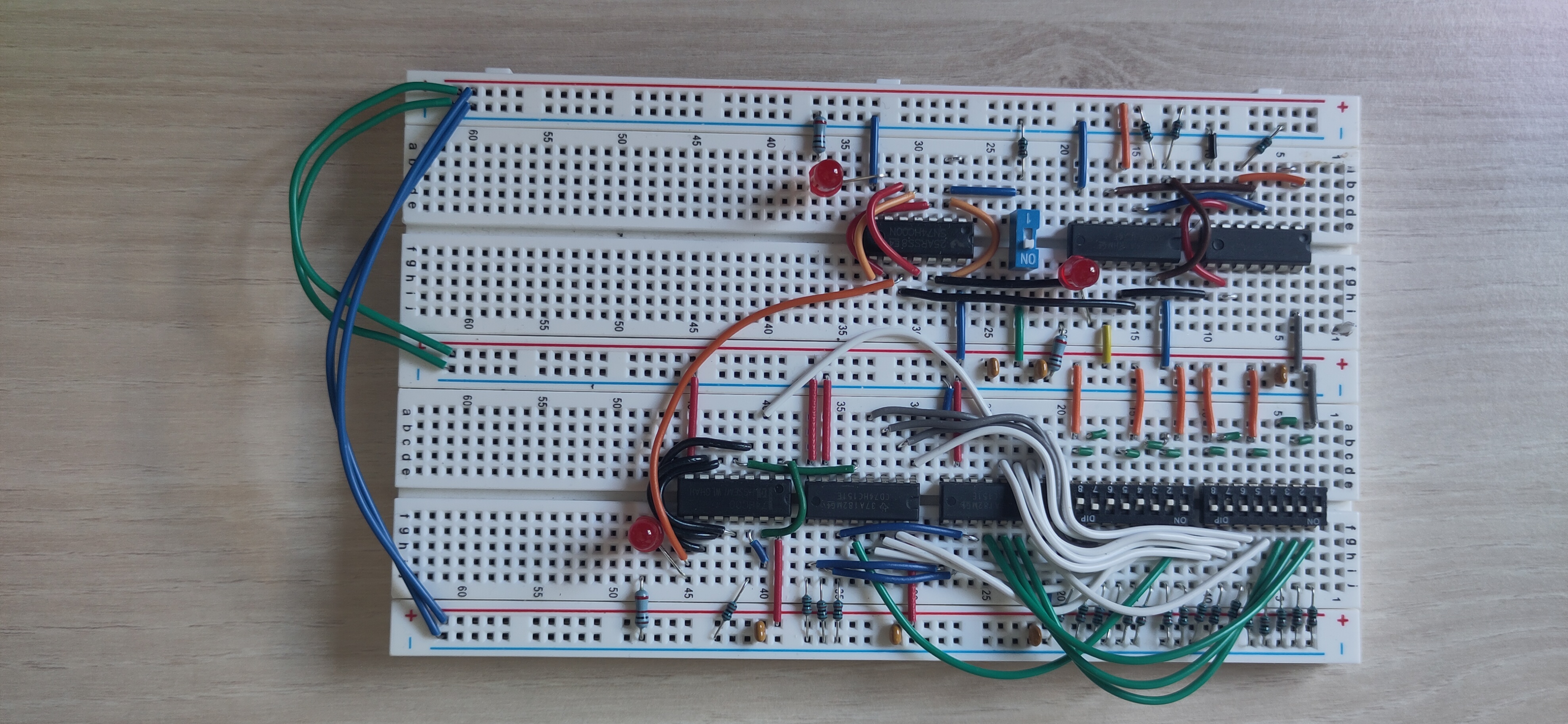
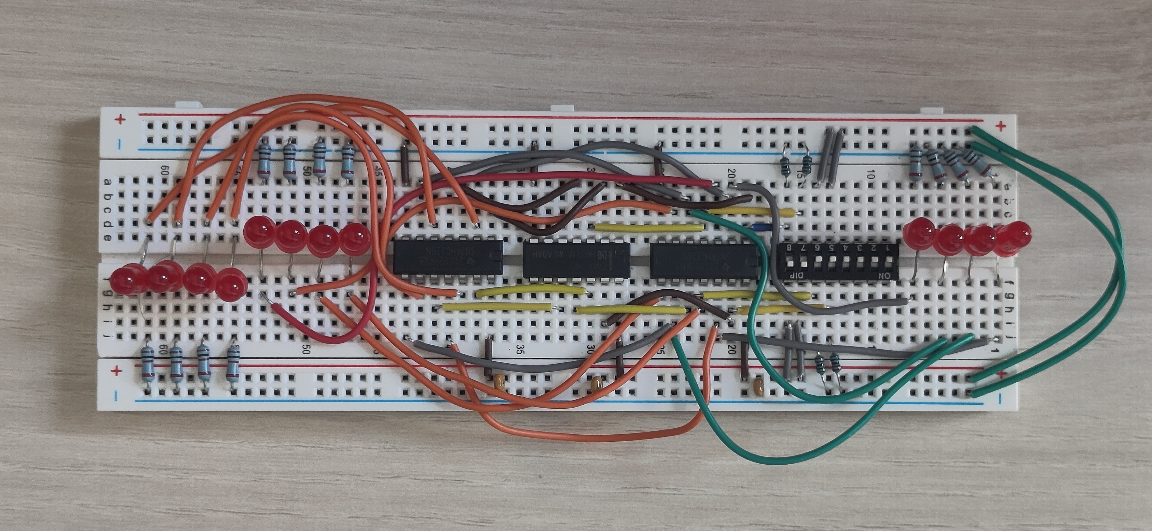
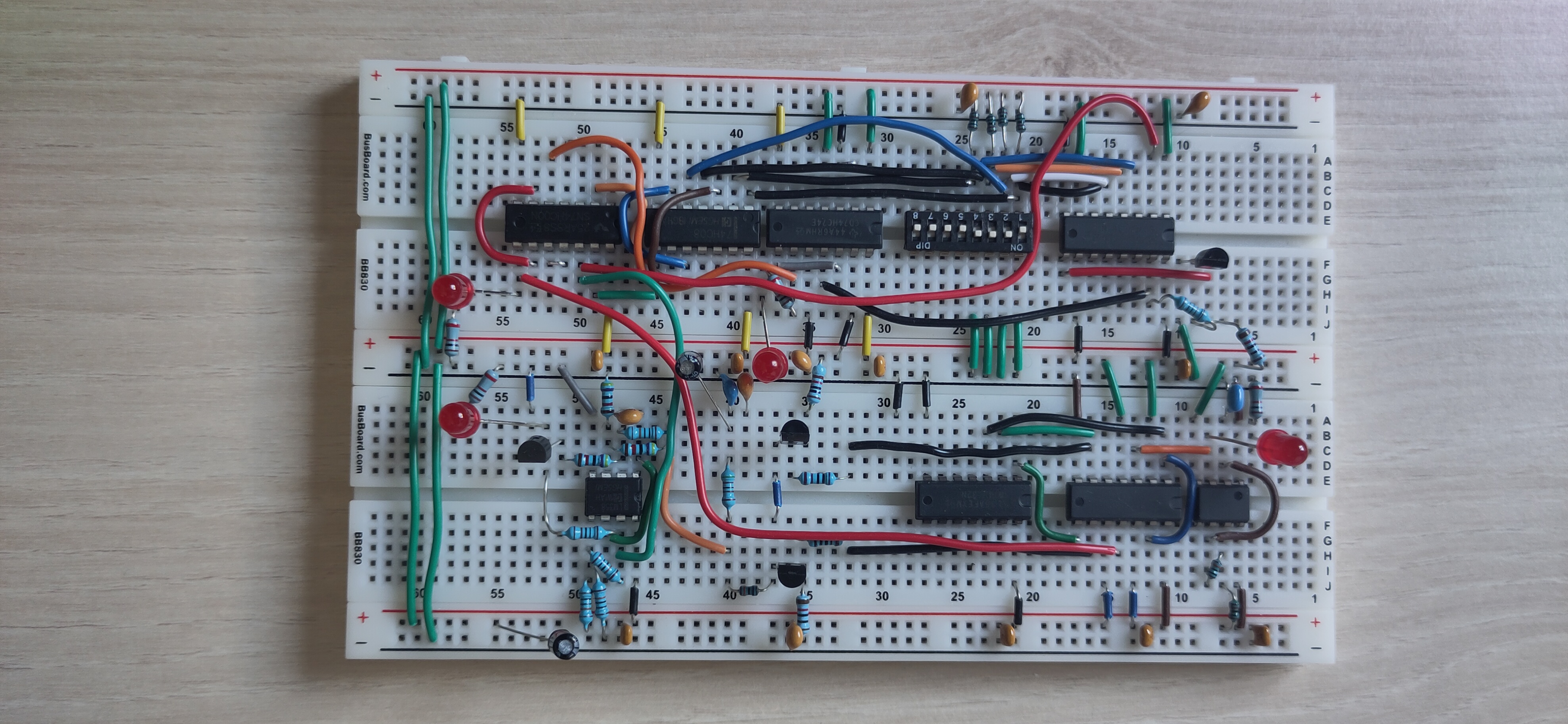
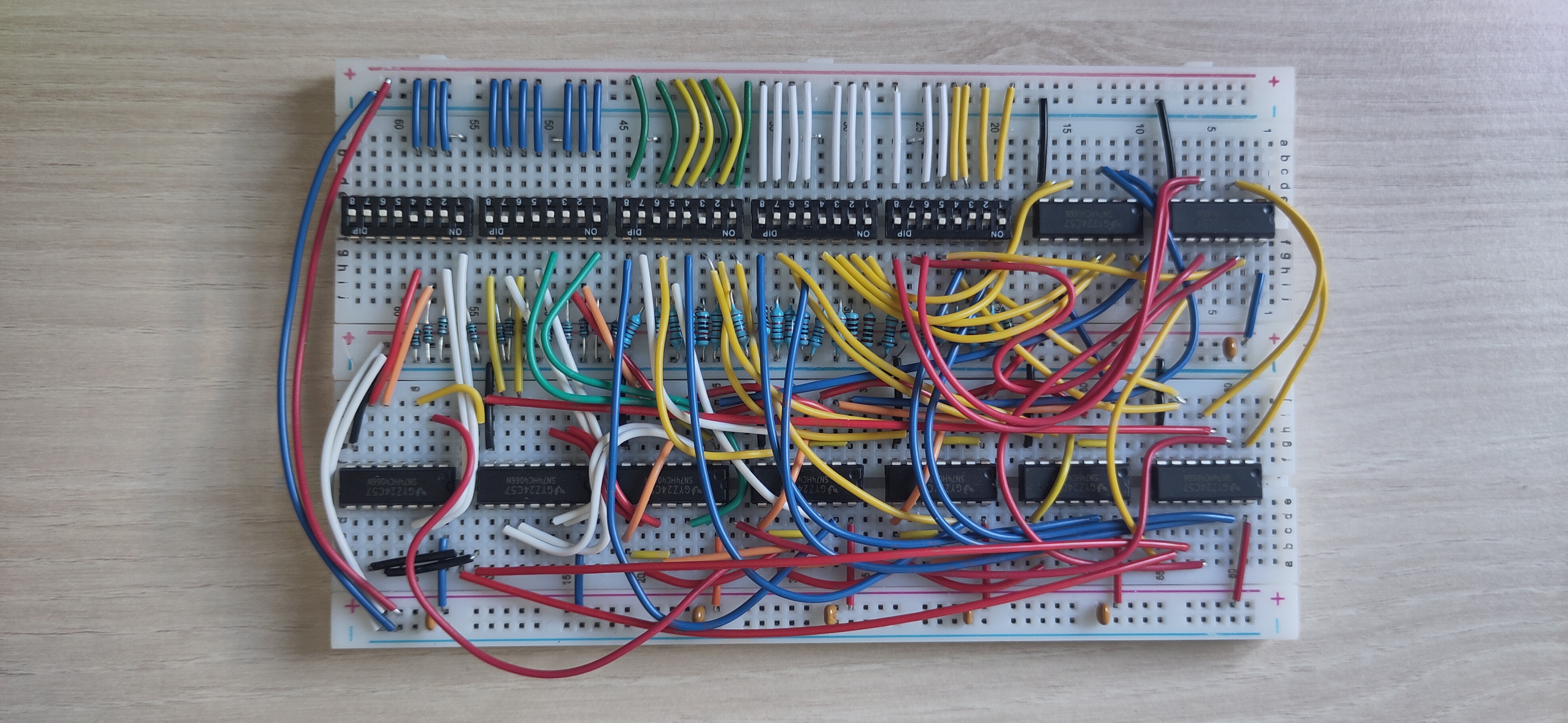
This is a fully custom (work in progress) minimal FPGA design. It consists of a Configurable Logic Blocks (CLB), a General Purpose Input/Output (GPIO), an Interconnect, and a Phase Lock Loop (PLL). I have built one of each of these at the moment and plan to build more of each in the future. Other than the PLL they are fully functional, but there are a few minor changes I would like to test before moving to PCB’s. Each of the independent circuits within the PLL are currently working but it’s not working correctly when they are all connected together.
Once I am happy with each of the modules, I plan on converting them to PCB’s and expanding the FPGA to contain more than 1 of each module so that it can perform some very basic operations. There is a more in depth explanation of each of the module in the posts below.